Introduction to Field Effect Transistor
| ✅ Paper Type: Free Essay | ✅ Subject: Physics |
| ✅ Wordcount: 1737 words | ✅ Published: 09 Mar 2018 |

To sir Mateen Yaqoob
Group Members
Maira Naseer
Aqsa Mahmood
The University of Lahore
Sargodha, Pakistan
Introduction to Field Effect Transistor
Transistor:
The word transistor is the short form of transforming resistor. Transistor is the special kind of resistor.
Resistor whose value changes, based on the input signal, and the resistor changes is transformative.

DEFINITION OF FIELD EFFECT TRANSISTOR:
The field effect transistor is a transistor which control the shape by using field effect transistor
Field effect transistor (FET):
In 1926 julius Edgar Lilienfeld was first patented the field-effect transistor and by Oskar Heil in 1934. But transistor effect was explained and oberserved by the team of william shockley at Bell labs in 1947 after it practical semiconductor were developed.
The field effect transistor and the PN junction:
The behavior of the field effect transistor hinges on the behaviour of a PN junction that is reverse biased. semiconductoris a material that is not a good conductor and not a good insulator but that when heat, light or voltage is added it conduct more electricity. which has two type ‘P type ‘and ‘N type’.
P type and N type material:
From type p material that has abundance of positive carriers, we called them holes to the type N material that has abundance of negative carriers, we called them electrons. By the way it’s not that the P material is positively charged and N material is negatively charged ,they both are electricallyneutral. The difference is that the p material has free to move positive carriers and N material free to move negative carriers.

PN Junction:
Formally we put P type and N type together and we form one we called PN junction. 
The PN junction was found to very interesting electric properties. It allowed to current to flow from p to n and when blocked current they try to move backward.


Forward biased p-n junction:
Now look at how p-n junction works when we try to pass current forward trade from p to n.
We apply voltage source across a p-n junction such that p-side is positive and n-side is negative ,then this voltage source tries to get current into the p material which effectively means that it pulling out electrons out of the left of p material and by doing that its creating new holes of the left side of the material which increasing the density of holes on the left side of the p material. That source at the same time is pulling current from the right of the n material which is equivalent to saying it to feeding new electrons into the right of the n material which increasing the density of free electrons on the right side of the n material. Observe there is high density holes on the left of the p material and there is high density of electrons on the right of the n material. Is that the gradient of density will move holes towards the right and electrons to the left and they will joining in the center and recombine and disappear. The motion of the holes is facilitated by electric field created by external source. This is the way the p-n junction operates when it forward biased and this process is continuous forever.

Reverse biased p-n junction:
Now look at how p-n junction works when we try to pass current reverse biased from n to p.
We apply voltage source across a p-n junction such that the negative terminal is connected at the p side and positive terminal is connected at the n-side ,then this voltage source tries to take current out of the p material which effectively means that it tries to feed electrons on the left of the p material, if we do that those electron are recombine with some of holes on the left of the p material and the density of holes will decreasing on the left side of the p material and holes disappears. That source at the same time is feed current into the n material and take electrons out of the n material which decreases the density of electrons on left side of the n material. Is that the difference of density in holes and electrons will gap the holes and electrons move away from the junction to even over the density of carries in p-n material when they do that is an uncovering some of the fixed charges near junction creating a region that is depleted of free charges so there is no carriers in this zone and this is a region that is stationary charges, negative on the p side and positive on the n side and these stationary charges stop the flow of current.


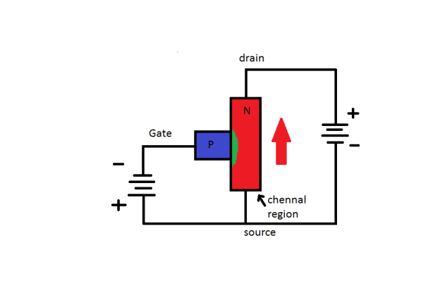
Basic information of FET’s :
Field effect transistor is the majority-charge-carrier devices, in which the current is carried mostly by majority carriers, or minority-charge-carrier devices. The field effect device consists of an active channel through which charge carriers flow from the source to the drain. Source and drain terminal conductors are connected to the semiconductor.
The FET’s three terminals are
Source (S):
Source S is the terminal through which the carriers enter the channel. usually, current entering the channel at S is identify by IS.
Drain (D):
Drain D is the terminal through which the carriers leave the channel. usually, current entering the channel at D is identify by ID and drain to source voltage is named as VDS
Gate (G):
Gate G is the terminal which set the channel conductivity.when voltage is apply on gate G it control the ID.
Type of FET’S:
Junction field effect transistor (JFET’S):
P type material and n type material is good conductor by themselves.so it’s possible to place two terminals on say the n material and get electrons to flow through a one end terminal to the other just like a wire and this is the basic junction field effect transistor. Electron flow through the n type region of p-n device from one terminal to the other and the name of this n region is the channel. The channel input is called the source and the channel output is called the drain. AND electrons flow from source to drain. The p type region of this device is called a gate. When there is no voltage applied to the gate electrons are completely free to flow to the channel so the source drain resistance is pretty much is zero ohms. When the JFETs is in this state we say it’s saturated, the channel electrons density is maximum.

However, when you reverse biased a gate an interesting thing happens. Reverse biased in the p-n junction causes a depletion region to appear just did in a diode and part of p and n material is convert back to being in insulator but now that depletion region causes the physical with the n channel to become narrow so less electron flow through the channel which rises resistance of the channel .
As we increase the negative voltage at the gate, the n channel become even more narrow and channel resistance rises further. If we increase voltage even further at some point the depletion will completely blocked the n channel, no current can flow across a channel and channel resistance is virtually infinite. At this point we say that the fact is cut off .Many also say that it is pinched off and the gate voltage pinched off the channel called the pinched off the voltage is around -4 volts. So this is how fact works, the reverse biased voltage of the gate causes channel resistance between source and drain to increase and it goes to infinite resistance at the pinched off voltage.

It’s possible to have channel made of p material instead of n material and we have a gate made of n material instead of p material. This is called a p channel JFET and it works exactly as the same way n channel JFET does accept the polarity are reversed .Electrons still flow from source to drain but this time the gate is reversed biased with positive voltage control in the channel resistance.

Difference between BJT and FET.
BIPOLAR JUNCTION TRANSISTOR:
- The full form of BJT is Bipolar Junction Transistor.
- The BJT is a current-controlled device since its output is determined on the input current.
- The basic construction of a BJT is two PN junctions producing three terminals.
- Bipolar junction transistor is high voltage gain.
- Bipolar junction transistor is Low input impedance.
- Bipolar junction transistor is low output impedance.
- Bipolar junction transistor is low input impedance.
- Bipolar junction transistor is medium nose generation.
- Bipolar junction transistor have medium switching time.
- Bipolar junction transistor requires zero input to turn off.
- Bipolar junction transistor is cheap.
- Bipolar junction transistor is easy to bias.
FIELD EFFECT TRANSISTOR:
- The full form of FET is Field Effect Transistor.
- Field effect transistor is a voltage-controlled device, due to its dependence on the field effect of the applied voltage.
- The field effect transistor construction does not have a PN junction in its main current carrying.
- Field effect transistor Is low voltage gain.
- Field effect transistor is high current gain.
- Field effect transistor is high input impedance.
- Field effect transistor is high output impedance.
- Field effect transistor is low noise generation.
- Field effect transistor has fast switching time.
- Field effect transistor requires some input to turn off.
- Field effect transistor is more expensive than BIPOLAR.
- Field effect transistor is difficult to bias.
Advantages of FET:
1: Field effect transistor is high input resistance which is 100 MΩ or more.
2:Field effect transistor is voltage-controlled device, and it show a high degree of separation between input and output.
3:Field effect transistor is depend on majority current flow and it is a unipolar device.
2: With shaping time base current will increase noise, and field effect transistor produce less noise as compare to bipolar junction and it is found in noise sensitive electronics.
Disadvantages of FET:
1: field effect transistor has low gain-bandwidth product as compared to a bipolar junction transistor.
2:. When reisitance is “on” field effect transistor is low and when resistance is “off” field effect transistor is high and field effect transistor can vanish large amount of power during switching.
Uses of FET:
1:.MOSFET is the most commonly used in field effect transistor 2: Field effect transistor used as an amplifier ,because it has large input resistance and low output resistance. FET’S effective as a buffer.
Page 1 of 9
Cite This Work
To export a reference to this article please select a referencing stye below:
Related Services
View all


DMCA / Removal Request
If you are the original writer of this essay and no longer wish to have your work published on UKEssays.com then please click the following link to email our support team:
Request essay removal