Mobile Sensor Network for Indoor Environment
| ✅ Paper Type: Free Essay | ✅ Subject: Engineering |
| ✅ Wordcount: 2514 words | ✅ Published: 31 Aug 2017 |
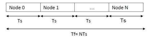
- 4 node sensor network without collisions.
- Update of every sensor reading in the network at least once per second (available from all nodes).
- Single frequency channel (i.e. no frequency multiplexing permitted).
- Error checking (CRC) included to (< 1/1000 false readings).
- Measure at least 2 parameters (e.g. temp, light..)
- Data presented on serial I/O port in a format that is easily readable on a text terminal.
1. Background knowledge
1.1. System structure
The aim of this coursework is to design a mobile sensor network for an indoor environment, communicating with a 2.4 GHz wireless link (IEEE 802.15.4). All the sensor nodes can realize data link, which means each board can get others information. All the sensor boards have the function of receiver link to the computer, and can present the sensor data (for all nodes in the network) to the serial I/O port in a format which is easily to be understand on a text terminal. If the nod which connected to pc is broken, the other 3 nodes can replace it and realize the function of receiver. Each sensor node will include a number of sensors interfaced to a microprocessor (for our group temperature, sounds, touch and light). The microprocessor will gather sensor data, communicate with other sensor nodes via a wireless transceiver, implement a network protocol and provide a PC interface via a serial I/O port for data display. The structure of whole system is as follow:
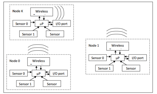
Figure 1 Architecture of Wireless Sensor Network
1.2. Basic hardware
The principle hardware used in this project is the PICDEM Z [3] development board from Microchip Technology Inc. There is a PIC18F4620 microcontroller on every node board and every group has 4 board available. The PICDEM Z has a prototyping area which must not be used for circuit construction. First, we need veroboard to construct a circuit, then interface it to the header J6. The next figure shows the structure of the board.
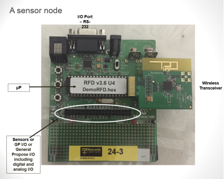
Figure 1 The structure of the board
And we also have other devices can use in this course:
1. 9V DC power socket (J1) for operation from mains adaptor.
2. 9V battery terminal (BT1) for mobile operation.
3. ICD connector (J5) for connection to MPLAB ICD3 in-system programmer/debugger cable.
4. RS232 serial port connector (P1) for connection to PC COM port.
5. Microchip MRF24J40 2.4GHz transceiver module connected to J2.
6. LEDS RA0 and RA1 for indication.
7. Push buttons RB4 and RB5 for simple logic input.
8. Header J6 giving access to analog and digital I/O pins Vcc (3.3V) and GND. This may be used to interface additional sensors.
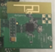
1.3. Microchip MRF24J40 2.4GHz
The MRF24J40 wireless transceiver [5] provides the physical layer for your wireless communication network. This is a 2.4GHz (IEEE 802.15.4 compliant) device which transmits data rates up to 250kbps and is connected to the PIC via SPI bus, as well as a small number of digital I/O pins. The picture of Wireless transceiver is as follow.
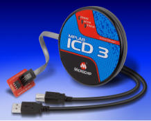
1.4. MPLAB-ICD
MPLAB-ICD is an inexpensive development tool for MICROCHIP’s PIC16F87X series MCU. MPLAB-ICD is an online debugger, and a programmer. It works in the MPLAB-IDE integrated development environment, and use online serial programming technology of MICROCHIP (In-Circuit Serial Programming), the monitoring program is embedded to achieve real-time simulation in the simulation of the MCU (PIC16F87X). The simulation head is directly connected to the MCU socket of the application system, running the user’s application as a PIC16F87X. The picture of MPLAB-ICD is as follow.
1.5. Wireless sensor network
Wireless Networks use radio waves, infrared, or any other wireless media to link to any devices. It can cover a large area, in which case it will be called a Wireless WAN, or it can cover an area or some floor of building, such as school, hospital and railway station, in that case Wireless LAN (WLAN) appear and describe the situation[4]. It appears a large number of wireless communication standards nowadays, including ZigBee, Wi-Fi, WiMax, GSM (Global System for Mobile Communications) et al.
Wireless sensor network (background) became a more and more popular way to solve the problems of large-scale tracking and monitoring applications because it has low-data-rate, low-energy-consumption, and short-range link network [1]. It give people a chance to monitor and control the physical world in a more simple way. WSN applications include many ways in our life, such as industrial monitoring, security, electronics industry, military sensing, asset tracking and home automation. WSNs research has mainly pay attention to energy consumption, routing and data transmission, ‘particularly focusing on collecting and data summary in specific networks with an associated sink node, called a WSN gateway’ [1].
Some research has carried out the interface of different sensor networks for a single or complex applications. Wireless sensor networks is aimed to monitor and control the physical data of environmental conditions at remove locations and it can collect their data to a main location and send their control command to achieve the result of remote control.
A WSN includes plenty nodes, ranging from a few to hundreds and thousands, in addition each node may be linked to one or more other nodes. One node can be designed for carrying out one or more different sensors which have various functions and we can also design combined sensors choice to complete complex use or exchange data with another network[4]. A node for sensing is called a sensor node, everyone can collect the data of other sensor node. As a result, any place with a sensor node can get all the data with a very fast speed at any time.

1.6. Error detection – Cyclic Redundancy Check
Error detection segment is necessary in a data transmitting system since the correctness and efficiency of data transmitting must be ensured. In this project, there are 3 approaches which can be applied to error detection: parity bit, check sum and cyclic redundancy check (CRC).
Parity bit is also known as check bit, the function of which is to judge whether a number of 1-bits in the string is even or odd by adding a bit to a string of binary code. The realisation is that the bits with value 1 is counted for even parity while the coding reverses for odd parity. Although parity bit is easy to implement, the shortcoming is apparent that only when there are 1, 3, 5, … bit(s) errors can the error be detected.
The principle for check sum is to define a string with a small size with designed algorithm of calculating, and the result of the calculations of before and after the transmitting will be different even the data changes slightly so the error could be detected in this way. Similar to parity bits, the disadvantage of check sum is that error can’t be detected under some circumstances.
Cyclic redundancy check (CRC) is a method of error detection that is easyto be implemented by shift register and look-up table in S/W. The process is shown in figure1.
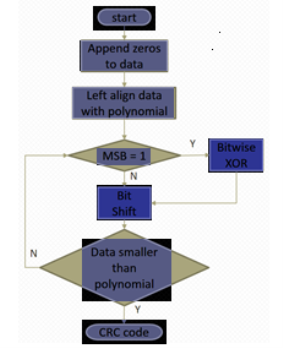
In this project the value of P(z) is 0x91 (11001 in reversed binary) which is known as generator polynomial and the divider. Assuming that the data needed to be transmitted is 110011000, then we have the message polynomial D(z). C(z) is the remainder which is calculated by D(z) divided by P(z). The realization of division operation is by XOR. Only when the least significant bit of 1 byte of the message is ‘1’ will it XOR with CRC polynomial, then we should shift it to the next bit and repeat the XOR. At the transmitter, the string of CRC depends on the whole frame on a bit-by-bit basis with binary division. And at the receiver, the received bit string is again divided by the same bit-by-bit basis with a serial shift register. The resultant CRC result should be all zeros at the end of the frame, or there must be errors in the process of data transmitting. Grahame Smillie, 10 – Bit error detection and correction, In Analogue and Digital Communication Techniques, Butterworth-Heinemann, Oxford, 1999, Pages 185-230, ISBN 9780340731253, http://dx.doi.org/10.1016/B978-034073125-3/50012-7.
2. System Design
2.1. Sensor design and calibration and Analogic digital converter – ADC
In our group 4 kinds of sensor are designed to meet the requirement, and they are temperature sensor, light sensor, touch sensor and sound sensor. In order to obtain data from all the 4 sensors in the wireless network, a PCB board is required to connect to the sensor node board. In the lab, a breadboard is available for testing the circuit. When finishing the circuit on the breadboard, it can be interfaced to PC to have a preliminary test. If done, a PCB board will be used to finish the final product which can connect to node board.
The method of calibration is to get the value of light, sound, temperature or touch that is detected using physical measurement. For example, if the temperature of the environment T0 and the result of the ADC conversion D0 that collected by the sensor in the same testing environment are known, we can derive the proportional function of temperature and ADC data with another pair of coordinate (T1, D1), which is obtained by changing the temperature of testing. Then the code that controlling display of temperature value should be modified so that by the time the temperature of the environment changes, the displaying value on the PC is exactly the temperature.
Code for this part is shown as following:
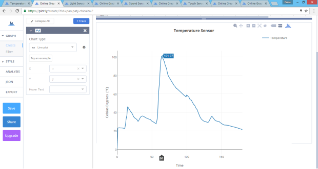
2.1.1. Temperature sensor
Negative Temperature Coefficient (NTC) thermistors are temperature sensitive semiconductor resistors which decrease in resistance value when absolute temperature increasing. Change in the resistance of NTC thermistor can be brought about either by a change in the ambient temperature or internally by self-heating resulting from current flowing through the device. (“NTC Thermistor Discs and Chips | Ametherm”, Ametherm, 2017. [Online]. Available: http://www.ametherm.com/thermistor/disc-and-chip-ntc-thermistors. [Accessed: 07- Jan- 2017].)
Most of the practical applications of NTC thermistors are based on these material characteristics. Time and temperature are two of the most frequently measured variables. There are various ways to measure temperature electronically, most normal is by thermocouples and negative temperature coefficient (NTC) thermistors. In addition, NTC temperature sensors can operate over a wide temperature range (-55 to +300°C). They are stable throughout a long time, and are small and cheaper than other kind. [3]
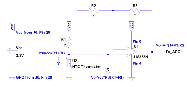
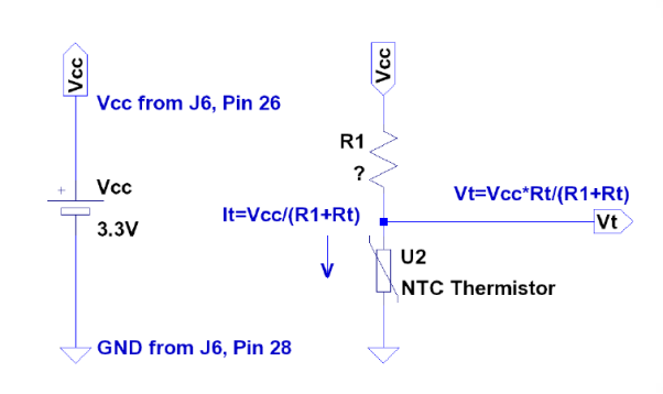
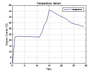
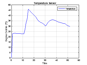
Figure 1 circuit of Temperature Sensor
It can be seen in the figure 1 that temperature Sensor is a more complex circuit design. On the left part It=Vcc/(R1+Rt) and Vt=Vcc*Rt/(Rt+R1), then connect the line to the positive side of the LM358 amplifier to amplify circuit and Vt becomes the input of the amplifier. After that, use formula
V0 = Vt*(1+R3/R2) to get the voltage value of v0. From this formula we can know, the value of V0 depends on R3 and R2, so R3 and R2 are both simply chosen 10 Ohm. Then the voltage value of V0 is exactly twice as much as that of Vt.
Next use formula to transfer ADC data to temperature, when it comes to the lab temperature (23 degrees Celsius), ADC data is 613. While it comes to the people body temperature (abort 38 degrees Celsius), ADC data become 530. Finally, we can calculate the linear parameters by these two sets of data.
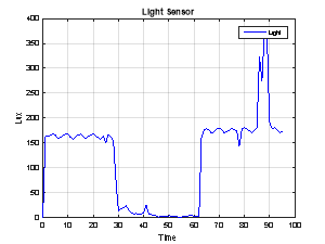
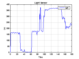
2.1.2. Light sensor
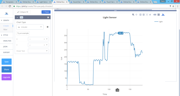
The Light Sensor is a passive devices that transfer “light energy” visible or invisible into a output of voltage signal. Thus Light sensors are more commonly known as “Photoelectric Devices” or “Photo Sensors” [2].
Photoelectric devices can be classified into two main categories, those which generate electricity when illuminated, such as Photo-voltaics or Photo-emissives etc, and those can change their electrical data (voltage) in some way such as Photo-resistors or Photo-conductors. [2]
Light sensor is the easiest sensor of our 4 sensor, so we also use the simplest structure, when luminance become strong, the value of photosensitive resistance become larger. Thus the voltage of Vt increase which result in the raise ADC data.
Then use formula to transfer ADC data to luminance, when it is dark (lux 0), ADC data is 30. While it comes to the lab light (about 330 lux), ADC data become 895. Finally, We can calculate the linear parameters by these two sets of data
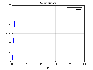
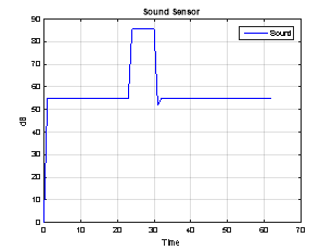
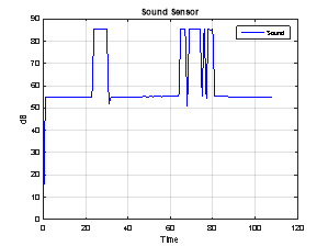
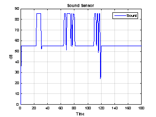
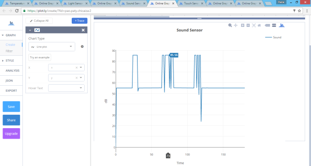
2.1.3. Sound sensor
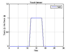
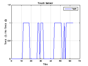
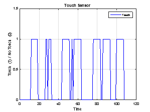
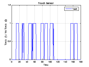
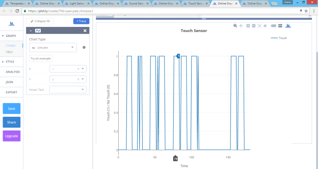
2.1.4. Touch sensor
The MPR121 is the second-generation sensor controller after the initial release of the MPR03x series devices. The MPR121 will feature increased internal intelligence in addition to Freescale’s second generation capacitance detection engine. Some of the major additions include an increased electrode count, a hardware configurable I 2Caddress, an expanded filtering system with debounce, and completely independent electrodes with auto-configuration built in. The device also features a 13th simulated electrode that represents the simultaneous charging of all the electrodes connected together to allow for increased proximity detection in a touch panel or touch screen array [5].
2.3. Time Division Multiple Access – TDMA
It is required that there are at least 4 nodes of sensor without collision in a wireless transmitting network based on a certain channel. Each sensor must be ensured to be able to receive and transmit, in other words, each node can serve as both a receiver and a transmitter. The node which connects to the PC is responsible for the display of the data that collected by each sensor and each sensor is supposed to send the data string to the chosen node within 1 second.
There will be collision with the four nodes if we don’t define the order of the data transmitting and receiving or just simply define by applying time delay, hence TDMA is necessary to meet requirements above. TDMA is a method of communication technique that derived from the P2S (parallel to serial) conversion. In the process of TDMA of this project, receivers obtain a same signal at the same time but only the appointed receiver reacts and does the next action, which is then transmitting and serving as new transmitter, and the new transmitter will wait for the next appointment without doing nothing unless it is appointed once again, which means it gets the same order in a new loop. The process repeats and there will not be data collision in the transmitting and receiving.
As is illustrated in figure2, there are 4 nodes so 4 slots are needed in 1 second according to the requirement, hence each slot takes up 0.25 second, during which time of period each node should finish data transmitting, so the calculation of the time that is needed for sending and receiving is necessary.
2.3.1. Data packet structure
2.3.2. Timers
We apply timer0 to control the time of running, different initial values have been given to timer0 in each slot so that transmitting and receiving within 1 second without collision can be ensured. In this case, node 4 is the main node which connects to the PC. The start of the process is the transmitting of node 4, and by the time other 3 nodes receive data from node 4, the text packet ID of the transmitter will be checked and only node 3, which is the transmitted ID 4 minus 1, will display the data that collected by node 4 and transmit its own data collected by its sensor. Following actions will be carried out by node 2, and node 1 within a certain time of period, like shown in figure3.
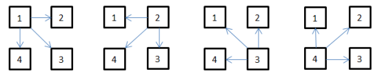
Figure3
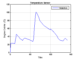
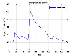
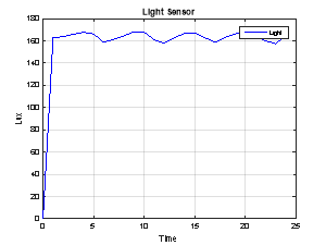
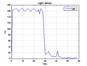
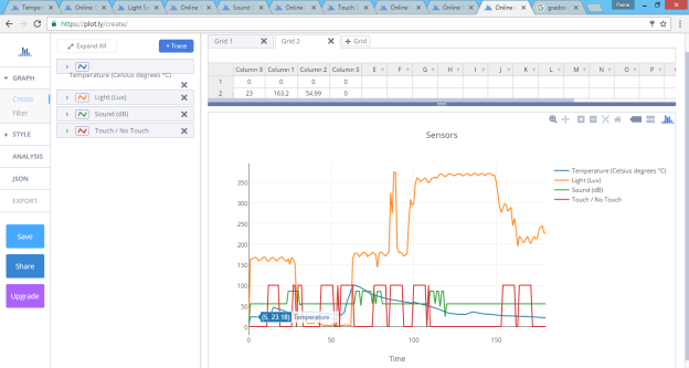
4. IoT Data Service and Visualisation
|
|
|
|
|
|
|
|
|
|
|
|
|
|
|
|
|
|
|
|
|
|
|
|
Cite This Work
To export a reference to this article please select a referencing stye below:
Related Services
View all


DMCA / Removal Request
If you are the original writer of this essay and no longer wish to have your work published on UKEssays.com then please click the following link to email our support team:
Request essay removal