Artificial Intelligence Chips & Comparison with CPUs and GPUs
| ✅ Paper Type: Free Essay | ✅ Subject: Computer Science |
| ✅ Wordcount: 3305 words | ✅ Published: 26 Oct 2021 |
ABSTRACT
With the rapid growth of artificial intelligence and machine learning algorithms, there is an ever-increasing demand of processors with high performance and low power consumption. To execute machine learning (ML) algorithms in less time, high computing power is required that can perform the basic operations of ML algorithms efficiently and in less time. Since the machine learning algorithms involve complex mathematical calculations, processors are being designed to perform these computations in a single clock cycle to train the model quickly. This paper discusses various processors that have been used to implement machine-learning algorithms. The paper further discusses the need for application-specific processes, followed by an example of Artificial Intelligence (AI) Accelerator i.e. Tensor Processing Unit (TPU). The paper concludes with a brief comparison between the central processing unit (CPU), the graphic processing unit (GPU) and the AI accelerator.
Keywords: Artificial Intelligence (AI), AI chip, AI accelerator, machine learning, tensor processing unit, neural network.
1. INTRODUCTION
In view of the increasing volume and range of available data, the need for statistical analysis is becoming essential for the delivery of in-depth information that is cheap and readily available. By using artificial intelligence and machine learning, algorithms that can process larger, more complex data can be programmed to produce faster and more accurate results. By determining the specific models to avoid unknown risks, companies are finding lucrative opportunities to grow their business. These algorithms help the companies to bridge the gap between their services and customers with better decisions and less human intervention [1].
Artificial Intelligence can be defined as a wide-ranging branch of computer science concerned with building smart machines capable of performing tasks that typically require human intelligence [2]. Building expert systems that can advise its users and developing systems that can exhibit human-like behavior are the main goals of artificial intelligence systems. Figure 1 enlists the different ways to develop artificial intelligence systems. The fields described in Figure 1 perform a large number of computations to train a system with large data sets, to execute a large number of computations; the system requires high computing power. Therefore, when developing AI systems, computing power becomes a limiting factor. E.g. In order to recognize a cat in a photo, it may be appropriate for a deep learning algorithm to see millions of images before its artificial neurons “remember” to recognize a cat. Therefore, chips explicitly for the artificial intelligence field are designed to accelerate the development of AI systems in order to provide higher performance when executing complex computations and consuming low power.

Figure 1. Fields of Artificial Intelligence
2. HISTORY FOR AI ACCELERATION
With the increasing demand and popularity of artificial intelligence and machine learning post the second AI winter [4], various processors and microcontrollers were used for acceleration of developing AI systems and machine learning models. As deep learning and machine learning workloads rose in prominence within the 2010s, specialized hardware units were developed or tailored from existing hardware to accelerate these tasks.
In the 1990s, digital signal processors were used as neural network accelerators and FPGA-based (field-programmable gate arrays) accelerators were developed to explore their use for training and inference [3]. In the 2000s with the advent of central processing units (CPUs) that have features beneficial for developing artificial intelligence systems like fast access to memory, arithmetic, and logical computing, etc. replaced the digital signal processors to function as neural network accelerators. Graphics Processing Units (GPUs) are electronic circuits used for processing images, video, and animations. The mathematical foundation for neural networks and object processing is identical, resulting in the growing use of GPUs for machine learning tasks. Because of GPU’s increasing popularity in machine learning and artificial intelligence, they continue to evolve towards promoting machine learning and deep learning operations, both in training and inference [3].
To provide increased programmability and develop a dedicated inference accelerator with short latencies, fast code porting, and support for major deep learning frameworks, reconfigurable devices like field-programmable gate arrays (FPGA) and chips like application-specific integrated circuit (ASIC) can be used. Reconfigurable devices like field-programmable gate arrays (FPGA) make it easier to evolve the hardware based on the needs of the AI system. Although the performance of GPUs and FPGAs is much better than that of CPUs for machine learning, an application-specific integrated circuit (ASIC) can achieve a significant efficiency factor with a more specific design. Developing chips dedicated to deep learning or machine learning i.e. AI Chips will further boost the efficiency of developing AI systems.
2.1 Computational Paradigms in AI
Though developing AI systems is synonymous to traditional computing, they also need advanced computing technologies like:
Unstructured Data: The datasets used for developing AI systems or machine-learning models most of the time contain unstructured data such as image, video, voice. Therefore, the models must be trained by sample training, fitting and then the trained models must be used to process the data.
Parallel Processing: A large amount of computation is usually required for processing and training the model. The basic calculation is essentially linear algebraic operations, such as large matrix multiplication. Massively parallel computing hardware is more suited for such operations than traditional universal processors.
Near-memory computation: Parameters are huge, requiring enormous storage capacity, high bandwidth and low memory access capacity for latency. Localization of data is prominent and suitable for the reuse of data.
3. ARTIFICIAL INTELLIGENCE CHIPS
AI chips or AI Accelerators are application-specific processors that are designed for training machine learning models and using these trained models for inference. AI Accelerators are less general-purpose as compared to GPUs. However, it excels at computing matrix multiplications; neural network layer’s output error and propagating the computed error to the neighboring layers. Furthermore, the AI accelerator reduces the time required to develop an AI system as compared to CPUs and GPUs. The majority of AI accelerators or chips are designed using FieldProgrammable Gate Arrays (FPGA) or using Application-Specific Integrated Circuits (ASIC).
In an environment transitioning to workload-optimized AI systems, companies will be more inclined towards the fastest, most flexible, most power-efficient and lowest-cost hardware technology, to execute their artificial intelligence or machine learning tasks including development, learning, and inference. The numerous AI chip-set architectures available in the market represent the diversity of machine learning, deep learning, natural language processing, and other AI workloads ranging from storage-intensive training to compute-intensive inference. In order to address the variety of workloads used to support AI chipsets, manufacturers combine a wide range of technologies in their product portfolios and even in embedded AI implementations.

Examples of AI Chips are Google Tensor Processing Unit (TPU), Intel Nervana, Qualcomm AI Chip, LG Neural Engine and AWS Inferentia.
4. TYPES OF AI CHIPS
Artificial Intelligence chips being highly specific in their operations require a more specific and customized architecture that can perform complex computations and meet the computational paradigms in AI. Thus, to develop AI chips, two of the most used circuits are Field-Programmable Gate Arrays (FPGA) and Application Specific Integrated Circuits (ASIC). Both of these circuits can be used to model different types of AI chips depending on the application and the system specifications.
4.1 ASIC as an AI Accelerator
Application Specific Integrated Circuit or ASIC is an integrated circuit that is designed to serve a highly specific purpose rather than performing several general-purpose operations [6]. Despite ASIC’s high cost, they can be tailored to match the exact requirements of the product and reduce the need for integration of additional components.
The major advantages of using ASIC are they are small and hence reduce the use of excess components. ASICs consume less power as compared to other circuits and provide higher performance. As a large number of circuits are built on a single chip, these aides to make high-speed applications. They are also highly efficient in their specific application.
A major disadvantage of ASIC is since they are customized; their flexibility for programming is low. Since the chips are designed from the root level, their cost per unit is high. ASIC chips also have a larger time to market margin.
4.2 FPGA as an AI Accelerator
All processors are called integrated circuit i.e. electronic circuits integrated on a silicon chip. Usually, the circuit is fixed when the chip is designed. A field-programmable gate array or FPGA is a type of chip that allows the end-user to reconfigure the circuit after it has been designed by programming it as required. The FPGA constructs a logical circuit, which can be reconfigured by connecting or disconnecting different parts of the circuit engraved on the silicon chip. FPGAs consist of a number of programmable circuits that can independently perform a small amount of computation and contain a programmable interconnect that connects these programmable circuits together. Due to the array of programmable circuits, the FPGA can perform a large number of parallel operations [7].
The advantages of using FGPA as an AI accelerator are they consume less power as compared to CPUs and GPUs. It is cheaper to program an FPGA rather than design an ASIC circuit. An FPGA is cheaper as compared to the cost required to design an ASIC.
Table 1 given below provides the major differences between an ASIC circuit and FPGA [8].
Table 1. Difference between FPGA and ASIC
|
FPGA |
ASIC |
|
Faster time to market – No layout or additional steps needed. |
Needs more design time to complete all the manufacturing steps. |
|
The area of the chip is large. |
The area of the chip is small. |
|
Slower and consume more power as compared to ASIC. |
Achieve higher speed and consume lower power. |
|
It can be reconfigured to fix bugs. |
It cannot be reconfigured once the chip is designed. |
|
The cost is lower for small volume as compared to ASIC. |
Suited for higher-volume mass production. |
5. TENSOR PROCESSING UNIT
Tensor processing unit or TPU is an application-specific integrated circuit developed by Google for the Tensor Flow machine-learning library and for training of neural networks.
5.1 Model of Neural Network
Neural networks are parallel computing devices, which is an attempt to make a computer model of the brain. The main objective is to develop a system to perform various computational tasks faster than traditional systems. These tasks include pattern recognition and classification, approximation, optimization, and data clustering [9]. Figure 2 given below depicts the model of a neural network that can be trained using the tensor-processing unit.
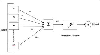
Figure 2. Model of a Neural Network
A neural network consists of an input layer, output layer, and one or more hidden layers. The input layer consists of inputs (x1, x2, …xm) and randomly selected weights for the corresponding inputs. In case of training, the inputs remain constant through the network and hence can be read only once. The weights of the corresponding inputs keep updating per cycle and for every layer hence the weights need to be constantly read and updated. The inputs and their corresponding weights are multiple and added to get the resulting sum of products of inputs and weights. This result is then normalized using an activation function and based on the normalized result; the output of the neural network is generated at the output layer. Here the summation of products of inputs and their corresponding weights is similar to matrix multiplication. Hence, AI accelerators designed for training neural networks require higher matrix multiplication computing power and storing the weights in a memory buffer from where they can be read and updated quickly while the inputs can be stored in a buffer and can be read once. In case of inference, the activation values are updated for every layer while the weights remain constant for a batch. Therefore the activation values need to be stored in a unified buffer while the weights determined while training the model can be stored in a slow-off memory.
5.2 Architecture
The TPUv1 was designed for a high volume of low precision computations. The TPUv1 was used developed only for neural network inference since the architecture was designed to perform a large number of low precision computations over a small number of high precision computations.

Figure 3. Floor Plan of TPU die (Yellow = compute, Blue = data, Green = I/O, Red = control)
The diagram above (figure 3) represents the floor plan of a TPUv1 die first introduced by Google in May 2016. The TPU is designed to act as an accelerator for complex computations like matrix multiplication. The TPU can be plugged into a host system and the host can send the instructions and data for which the computations need to be executed to the TPU. The results of the computations performed by the TPU are returned back to the host system via the same interface.
The Host Interface in a TPU is used to communicate with the host system. In this scenario, the TPU will accelerate the process of matrix multiplications while the host system can take care of other general-purpose operations that need to be performed to train the model. There are three different forms of data present in the TPU: weights are stored in DDR3 Memory, the activations are stored in Unified Buffer from where they can be read and updated quickly, and the control instructions are stored in the Control Unit.
The host needs to access the Unified Buffer quickly to read the output of inference and to write new inputs for computation. As seen in figure 3, a major part of the chip’s space (53%) is consumed by the unified buffer and Matrix Multiplication Unit (MXU) [10] [11].
5.3 Workflow of TPU
The diagram (figure 4) given below depicts the high-level chip architecture of TPU. The workflow of data and instructions is discussed in this section with reference to the diagram.
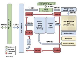
Figure 4. TPUv1 High-level chip architecture
During start-up, the unified buffer and DDR3 storage is empty. The host machine loads the training neural network model on the TPU; the weights of the model are placed in the DDR3 memory.
The host system fills the input values (activations) into the unified buffer. The control unit sends a signal to fetch the weights and store it in the Matrix Multiply Unit (MXU). Before computation of the next batch, the weights are pre-fetched into the Weight FIFO, this ensures that the next set of weights is prefetched while computing the current batch.
When the host system triggers the execution of the inference engine, the input values and weights are loaded into the MXU and the output of matrix multiplication is propagated to the Accumulators. The MXU writes back the updated activations back to the Unified Buffer via the Accumulators and then through the Activation Pipeline. The activation function of a neural network is present in the Activation module. The output of MXU is accumulated and the normalized activation value for the input values is computed. This updated activation values replace the old values in the Unified Buffer.
The above steps are repeated for all the hidden layers present in the trained neural network model. The activation values obtained in the last layer are sent back to the host system via the Host Interface.
The control flow in the above diagram is marked in red. The control unit takes the instructions from the host and ensures that the instructions are executed in the correct order. The control will take care of operations like when the MXU should perform matrix multiplication, selecting the weights that need to be prefetched, the time when the weights should be fetched into the Weight FIFO and the operations that the activation pipeline needs to perform based on the activation function. Hence the control flow is responsible for the proper execution of operations on the chip it acts as a captain for the rest of the chip. The TPU outperforms the CPU and GPU in performing linear algebra computations.
6. CPU vs GPU vs AI Chip
This section discusses the major differences between the various processors and it further explains the most suitable processor for developing AI systems based on the size of the system that needs to be designed.
6.1 Comparative Study
The diagram (figure 5) given below shows the major difference between the different processors i.e. CPU, GPU, FPGA, and ASIC. As seen from the diagram, as we move from generalpurpose processors (CPU) towards application-specific processors (FPGA/ASIC); the flexibility of the processor decreases and the efficiency of the processor to perform operations increases.

Figure 5. Flexibility vs Efficiency in different processors [13]
Thus, there is a tradeoff between flexibility and efficiency, in different processors. The CPU is a general-purpose processor that enables the user to perform a variety of operations through its efficiency is less. On the contrary, the AI Chips developed using FPGA/ASIC, can only perform the specific operation for which they are designed thus reducing the flexibility of the processor but these chips are highly efficient in performing complex machine learning computations [12].
Apart from flexibility and efficiency, another major factor is the performance of processors while developing machine-learning models. As seen in the diagram below, the TPU or AI Chip outperforms the CPU and GPU while performing predictions using a trained neural network model.
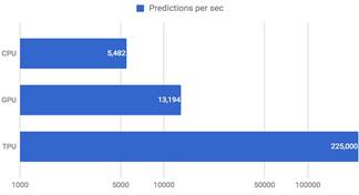
Figure 6. Performance comparison for Neural Network Inferencing
Another performance metric to compare the processors is the CPU can handle tens of operations per cycle, the GPU can handle tens of thousands of operations per cycle while the TPU can handle up to 128000 operations per cycle.
The table below outlines the major differences between CPU, GPU, and TPU.
Table 2. Comparison between CPU, GPU and TPU
|
CPU |
GPU |
TPU |
|
|
Executes a scalar operation per cycle. |
Executes a vector operation per cycle. |
Executes a tensor (matrix) operation per cycle |
|
|
Designed to solve the computational problems in a general fashion. |
Designed accelerate rendering graphics. |
to the of |
Designed to perform a specific task i.e. accelerate deep learning. |
|
Used for generalpurpose programming. |
Used for graphics rendering, machine learning, and general-purpose programming. |
Used specifically for training and inference of deep learning models. |
|
|
It provides high flexibility and low efficiency. |
It provides low flexibility and high efficiency as compared to CPU. |
It provides high efficiency and low flexibility. |
|
6.2 Selection of Processor
Choosing the ideal processor for developing an AI system is an important step since a large number of factors need to be taken into consideration. Performance, cost, dataset size, size of the model are a few parameters that need to be considered while selecting the ideal processor to develop a machine leering or AI system.
The figure below enlists the scenarios for selecting the ideal processor for developing systems of different sizes.

Figure 6. Speed-up Comparison
7. SUMMARY
As seen in the paper, AI Chips have a huge potential of revolutionize the development of AI systems and deep learning models. AI Chips provide higher throughput for developing machine-learning models as compared to other processors. With the increasing demand for machine learning and deep learning, chip manufactures can draw more number of customers by developing chips that can perform compute-intensive operations in lesser time and provide higher efficiency. Thus, AI chips will have a huge demand in the near future with the increasing complexity of deep learning models.
8. REFERENCES
[1] Paromita, Artificial Intelligence & Machine Learning: The Future Is Now! (https://analyticstraining.com/machinelearning-the-future-is-now/)
[2] What is Artificial Intelligence (https://builtin.com/artificialintelligence)
[3] AI-Accelerator (https://en.wikipedia.org/wiki/AI_accelerator)
[4] AI Winter (https://en.wikipedia.org/wiki/AI_winter)
[5] Tsinghua University, White paper on AI Chip Technologies (https://www.080910t.com/downloads/AI%20Chip%202018%20EN.pdf)
[6] ASIC (https://en.wikipedia.org/wiki/Applicationspecific_integrated_circuit)
[7] Machine Learning Accelerators (http://www.cs.cornell.edu/courses/cs4787/2019sp/notes/lec ture25.pdf)
[8] FPGA ASIC PCB comparison (https://anysilicon.com/whenand-why-should-you-choose-an-asic/asic-fpga-pcbcomparison/)
[9] Artificial Neural Network
(https://www.tutorialspoint.com/artificial_neural_network/artificial_neural_network_basic_concepts.htm)
[10] Anton Paquin. What’s inside a TPU?
(https://medium.com/@antonpaquin/whats-inside-a-tpuc013eb51973e)
[11] Kaz Sato, Cliff Young, David Patterson. An in-depth look at Google’s first Tensor Processing Unit (https://cloud.google.com/blog/products/gcp/an-in-depthlook-at-googles-first-tensor-processing-unit-tpu)
[12] CPU vs GPU vs TPU (https://iq.opengenus.org/cpu-vs-gpuvs-tpu/)
[13] What are field-programmable gate arrays (FPGA) and how to deploy (https://docs.microsoft.com/en-us/azure/machinelearning/service/how-to-deploy-fpga-web-service)
Cite This Work
To export a reference to this article please select a referencing stye below:
Related Services
View all


DMCA / Removal Request
If you are the original writer of this essay and no longer wish to have your work published on UKEssays.com then please click the following link to email our support team:
Request essay removal